Home/Exhibits/Digital & AI/From sand to chips

From sand to chips

From a handful of sand that can be easily lifted to an indispensable chip in various industries, it requires a very…

From sand to chips — Digital & AI exhibit for science museums
Reference image
CategoryDigital & AI
Standard sizeCustom size
SupplySingle unit or batch · OEM to your drawing
Lead timeStandard 4–8 weeks after deposit (confirmed per contract)
Warranty1 year, structure and control
DocumentsSpecification sheet · control diagram · spare-part list

A standard catalogue model: the dimensions, control package and finish are fixed, which is what keeps the price and the lead time predictable. Size, colour and interface language can be adapted without a new design cycle.

Ask about this model → Email us

Standard models from this range are also listed in our online store, priced in USD — see the price yourself ↗
01 / Overview

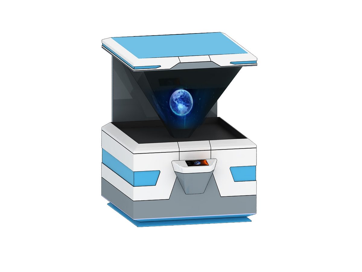
From a handful of sand that can be easily lifted to an indispensable chip in various industries, it requires a very complex processing program. one Extraction and purification of silicon 2 Making Silicon Ingots 3 Cutting silicon ingots 4 Photolithography 5 Etching and deposition 6 Testing and packaging.

02 / How visitors use it

The unit is designed for unsupervised public use: controls are recessed or shielded, moving parts are enclosed, and the interface is operable by a child of about six with no instruction. Where a screen is used, the language can be switched without changing the hardware, and the content can be replaced on site.

03 / The science behind it

The semiconductor material used in chips is monocrystalline silicon. Sand needs to be refined into pure silicon ingots with a purity of 99.99% or higher. After silicon melting, purification, high-temperature shaping, and rotation stretching, the sand will become monocrystalline silicon rods. After cutting, rolling, slicing, chamfering, and polishing, silicon wafers can be obtained, which are the basic materials for manufacturing semiconductor chips. The production process of monocrystalline silicon slicing involves more than ten techniques, mainly including slicing, chamfering, cleaning, polishing, testing, and packaging. Slicing refers to cutting a single crystal silicon rod into thin pieces with precise geometric dimensions. With this thin silicon wafer, we can truly enter the manufacturing process of integrated circuits. On each wafer, tens of thousands of chip circuits can be implemented, and each small cell on the wafer is a physical implementation of a chip circuit, called a grain. Observing the wafer under a microscope, it was found that the surface of the wafer was covered with crisscrossing 3D circuits. On the chip.

04 / Built for a public floor

Every unit leaves the factory after a running test: mechanisms cycled, electronics burned in, edges dressed, fixings torqued and marked. Wear parts — bearings, sliders, lamps, belts, touch panels — are modular and listed on the spare-part sheet, so a venue technician can replace them without returning the exhibit. Crating is plywood with foam blocking; the loading plan and packing list travel with the shipment.

Same category

More in Digital & AI

Other models from the Digital & AI line, all held to the same specification and the same control package.

Start a project

Send us your exhibit list.
We will come back with a price.

Attach a theme outline, a floor plan, or nothing at all — a photo of the space is enough to start. Quotations are issued against a real exhibit list, not per-square-metre guesses.

WeChat QR code — scan to message us Scan to add us
on WeChat